How it all began. The manufacturing of Integrated Circuit.
The first ever transistor was created by William Shockley, John Bardeen, and Walter Brattain from the Bell Labs at around 1947.

The first ever transistor. Big and ugly.

This is how a wafer filled with transistors look like today.
Now I'll give a brief graphical explanation on how an IC is manufactured.


This process is done many times until it satisfies the design which is set by the designer of the particular Integrated Circuit Chip.

The completed Integrated Circuit would look something like this internally.
The final step of the manufacturing process is the encapsulation process. The integrated circuit die is being encpsulated with ceramic, plastic, or epoxy to prevent physical damage or corrosion.

This is how the final product looks like.
Written by : Tan Ken Seong
Referred to:
Semiconductor fabrication, Wikipedia
http://www.madehow.com/Volume-2/Integrated-Circuit.html
Demetrios Papageogiou, Electrical Computer Engineering Department, Northeastern University.

The first ever transistor. Big and ugly.

This is how a wafer filled with transistors look like today.
Now I'll give a brief graphical explanation on how an IC is manufactured.
The integrated circuit is based mostly on pure silicon. Silicon is used as it's wafer which can keep thousands of transistors, resistors, diodes and such. Integrated Circuits are made by the hundreds at once time where a single large slice of silicon of wafer is made and then cut into individual IC Chips. The manufacturing has to be made in a clean room where the air is filtered from dust and foreign particles.

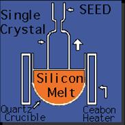
The melting process of a silicon.

Vacuum Chamber
The silicon is kept in a vacuum chamber where it is heated to about 1400C which is it's melting point. As the silicon mets, any impurities in the silicon becomes active. The heating coil is then slowly moved downwards to heat the other parts of the silicon in the chamber. The active impurities will follow the heating coil until it reaches the bottom of the silicon chamber. The bottom of the silicon layer is then sliced off and the rest of the cylindrical ingot is of pure silicon.

The Silicon Slicing Diagram.

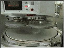
Silicon wafer is then polished to perfection.
Now that the silicon wafer is made, it can be modified such as patterning, deposition, and removal to determine the end result of the Integrated Circuit. Since the silicon wafer is so small and the cuttings in the wafer would be microscopic, the design for each layer of the wafer will be prepared in a computer-aided drafting machine, and the image will be made into a mask which will be optically reduced and transferred to the surface of the wafer. There are 2 methods of masking that can be used which is through contact and projection.
The mask are used on an aligner which aligns the mask to the wafer. The mask is then moved into the decided position and brought into contact with the wafer. An ultrviolet light then exposes the unprotected photosensitive material on the wafer surface.

The melting process of a silicon.

Vacuum Chamber
The silicon is kept in a vacuum chamber where it is heated to about 1400C which is it's melting point. As the silicon mets, any impurities in the silicon becomes active. The heating coil is then slowly moved downwards to heat the other parts of the silicon in the chamber. The active impurities will follow the heating coil until it reaches the bottom of the silicon chamber. The bottom of the silicon layer is then sliced off and the rest of the cylindrical ingot is of pure silicon.

The Silicon Slicing Diagram.

Silicon wafer is then polished to perfection.
Now that the silicon wafer is made, it can be modified such as patterning, deposition, and removal to determine the end result of the Integrated Circuit. Since the silicon wafer is so small and the cuttings in the wafer would be microscopic, the design for each layer of the wafer will be prepared in a computer-aided drafting machine, and the image will be made into a mask which will be optically reduced and transferred to the surface of the wafer. There are 2 methods of masking that can be used which is through contact and projection.
The mask are used on an aligner which aligns the mask to the wafer. The mask is then moved into the decided position and brought into contact with the wafer. An ultrviolet light then exposes the unprotected photosensitive material on the wafer surface.


This process is done many times until it satisfies the design which is set by the designer of the particular Integrated Circuit Chip.

The completed Integrated Circuit would look something like this internally.
The final step of the manufacturing process is the encapsulation process. The integrated circuit die is being encpsulated with ceramic, plastic, or epoxy to prevent physical damage or corrosion.

This is how the final product looks like.
Written by : Tan Ken Seong
Referred to:
Semiconductor fabrication, Wikipedia
http://www.madehow.com/Volume-2/Integrated-Circuit.html
Demetrios Papageogiou, Electrical Computer Engineering Department, Northeastern University.


0 Comments:
Post a Comment
<< Home