Image Hosted by ImageShack.us

Saturday, March 18, 2006

Finish Product.

After 9 full weeks, the project is finally completed. Here are the finish product.


The Dummy IC + Circuit.


The Dummy IC.

And also, we did a short documentary on how the IC would actually be used in application. Sadly some portion of the video the voice couldn't be heard clearly. Here's the video anyways.


Thursday, March 16, 2006

Prototype Completed. Poster Completed.

After spending 2 full days in the lab until late evening, the prototype and poster is finally completed. The prototype is fully working with the circuit and the poster has been designed and will be printed by this weekened to be presented.

On the 15th of March, the group done the soldering of the internal circuitry, fixing the IC legs and the IC Dye. Soldering was mainly done by Yang while the IC Dye was done by Tong Jiun. The cutting of the IC Legs as well as the IC connectors from the IC leg to the IC Dye was done by me.

On the 16th of March, the group started soldering the extended wires from the Circuit to the Real IC attachted to the bottom of the Dummy IC. Extended wires were needed as the current length of the wire was too short to display the Circuit properly. While I was helping Jin Yang with the soldering, Tong Jiun was working on the 2nd layer of the IC Dye. After that, we tested the IC Circuit and it worked. Apart from that, it is also discovered that the circuit would also work when it is conducted by a human body. This is because circuit only requires very little current to complete the circuit. However, this method does not work with everyone who tested by holding both terminals with separate hands. This is due to the difference of resistance in different human body and also the moisture of the contact point of the terminal and the human body. It is noticed that the more moisture the contact point is, the higher frequency of beeps is generated. Thus an idea was generated that this could actually be used as a gimmick to attract interest from regular people so that they would be more interested into knowing on how does an IC actually functions. The plan was to create a simple 'love-0-meter' that is able give responses when two people are holding each terminals while holding each other's hands. If the speaker is able to give a periodic beep then they are meant to be together. Else, they are not a good match. After the test, questions of how does this 'love-0-meter' work is highly expected. Thus, we are then able to move on to the details on how the IC actually works.


Tong Jiun Flattening the surface of aluminium.


Jin Yang glueing the connecters to on the Dummy IC surface.

I'm the cameraman! =]


This is the poster that has been designed by the groupmates.
Image Hosted by ImageShack.us

DCR (Dummy IC)

Image Hosted by ImageShack.us

Thursday, March 09, 2006

A Day at the Mechanical Workshop.

Yesterday the groupmembers Tong jiun, Jin yang and I stayed back to finish up what's left of the prototype construction. Most of the things done yesterday were the cutting of the arcylic as well as the soldering of the wires so that the real IC will be able to fit at the bottom of the Dummy IC. The arcylic will be used as the casing for the Dummy IC as well as to demosntrate the layers of wafer in an IC Dye. Tongjiun & I was in charge of cutting the arcylic while jin yang was in charge of doing the soldering works. there were no exact measurements for the arcylic case as the dimensions of the Dummy IC was not exact as there as a standard deviation of roughly 0.2mm. A hand saw was used to cut the arcylic. To make the case fit the Dummy IC, the arcylic was further sand papered to trim it's width & length a little bit.

Rough measurements of the arcylic sheet:
1 x [26.9x19.7] cm
2 x [26.9x7.2] cm
1 x [8x8] cm
2 x [8x2] cm

The finishing touch of the prototype will be done by tong jiun. jinyang and i will be working on the poster by the end of the week.


Jin Yang working on the soldering.


Tong Jiun cutting the pieces of arcylic.


That's me working on the arcylic as well.

Monday, March 06, 2006

Progress of the Project.

This will be a short post. The group has completed the presentation regarding the progress of the project. Feel free to download the presentation if you want to have a look at it. Link Here! The main part of the presentation is done by me but it is then seperate into 3 parts where me, jin yang and tong jiun are presenting individually where each group member edited the slides of their own section and then we combined all of them to make a full presentation.

Sunday, March 05, 2006

Change of Prototype Material.

After testing the prototype with the Plaster of Paris, it is found that the material is not suitable for the contruction of the Dummy IC. This is because the group faced many problems in using the material which are:

1. The prototype created is very uneven because there is no proper mould to make it. (shoebox was used)
2. The material is too heavy. This is cause problem during transportation as well as the contruction of the Dummy IC's legs.
3. The material takes too long to dry. After leaving the prototype in open air for a week. It is still wet. And thus not suitable for spraying colour.
4. Colour spray doesn not absorb evenly on the surface of the Dummy IC. This is related to the wetness of the surface of the Dummy IC.

After dropping the plans to build the prototype with Plaster of Paris, A new material is then chosen to construct the Dummy IC. Wood. These are the reaons why wood was chosen:

1. The surface of the prototype that is contructed is even this is because wood is properly cut flat.
2. The material although heavy, but it was not as heavy as the pervious prototype material which was Plaster of Paris
3. The material is ready for spraying immediately.


The prototype with it's leg placed for measurement.


The spacing between the wood to make way for the IC Dye and the insides of the Dummy IC

Thursday, February 23, 2006

Construction of Prototype

After some discussions regarding the anatomy of the integrated circuit has been discussed between jin yang and mushtak, the construction of the prototype of the integrated circuit has already began.

Items were bought from Vision Art &
3x 1kg Plaster of Paris
1x Uhu Glue
1x Paper Clay
1x Black Spray Can
2x Sand Paper

After that the we started the contruction of the main build of the integrated circuit.


Plaster of Paris (POP) with the mould which is actually a shoe box.


The mixture of POP is inserted into the mould.


The mould for the smaller parts of the Integrated Circuit.


After leaving the POP in the mould for a few hours, the mould is torn apart and this is what we get. The surface was rough so an extra layer was applied and it will be sand papered as well to get the texture that is equilavent to a read Integrated Circuit.


The finish product! Sand paper hasn't been used on it yet. The construction of the prototype will resume tomorrow.

Suprisingly today went pretty smoothly as there were not major setbacks in our construction other than chipped edges and the leakage of POP due to the mould not being airtight. The chipped edges was due to the extra POP that leaked through the mould that breaks the edges away as the mould was removed.

Design Change Request

This is the new Design Change Request that has been approved by Mr.Mushtak.
Image Hosted by ImageShack.us

Wednesday, February 15, 2006

How it all began. The manufacturing of Integrated Circuit.

The first ever transistor was created by William Shockley, John Bardeen, and Walter Brattain from the Bell Labs at around 1947.

The first ever transistor. Big and ugly.


This is how a wafer filled with transistors look like today.

Now I'll give a brief graphical explanation on how an IC is manufactured.

The integrated circuit is based mostly on pure silicon. Silicon is used as it's wafer which can keep thousands of transistors, resistors, diodes and such. Integrated Circuits are made by the hundreds at once time where a single large slice of silicon of wafer is made and then cut into individual IC Chips. The manufacturing has to be made in a clean room where the air is filtered from dust and foreign particles.

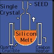
The melting process of a silicon.


Vacuum Chamber

The silicon is kept in a vacuum chamber where it is heated to about 1400C which is it's melting point. As the silicon mets, any impurities in the silicon becomes active. The heating coil is then slowly moved downwards to heat the other parts of the silicon in the chamber. The active impurities will follow the heating coil until it reaches the bottom of the silicon chamber. The bottom of the silicon layer is then sliced off and the rest of the cylindrical ingot is of pure silicon.


The Silicon Slicing Diagram.


Silicon wafer is then polished to perfection.

Now that the silicon wafer is made, it can be modified such as patterning, deposition, and removal to determine the end result of the Integrated Circuit. Since the silicon wafer is so small and the cuttings in the wafer would be microscopic, the design for each layer of the wafer will be prepared in a computer-aided drafting machine, and the image will be made into a mask which will be optically reduced and transferred to the surface of the wafer. There are 2 methods of masking that can be used which is through contact and projection. the contact masking method is usually used when the features are more than 1 micrometer and projection method is used when it's less than 1 micrometer.

The mask are used on an aligner which aligns the mask to the wafer. The mask is then moved into the decided position and brought into contact with the wafer. An ultrviolet light then exposes the unprotected photosensitive material on the wafer surface.

Image Hosted by ImageShack.us

Image Hosted by ImageShack.us

Image Hosted by ImageShack.us


This process is done many times until it satisfies the design which is set by the designer of the particular Integrated Circuit Chip.


The completed Integrated Circuit would look something like this internally.

The final step of the manufacturing process is the encapsulation process. The integrated circuit die is being encpsulated with ceramic, plastic, or epoxy to prevent physical damage or corrosion.


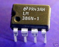
This is how the final product looks like.

Written by : Tan Ken Seong

Referred to:
Semiconductor fabrication, Wikipedia
http://www.madehow.com/Volume-2/Integrated-Circuit.html
Demetrios Papageogiou, Electrical Computer Engineering Department, Northeastern University.

Saturday, February 11, 2006

Problems Encountered.

After some serious considerations regarding the current design proposal for the circuit, the team members has decided to drop the design and will soon propose for a Design Change Request. Reasons for the changes are due to the complexity of the circuit and the time contraint faced. This will be explained in detail more in the DCR that will be produced and handed in very soon. Meanwhile, the new product that is to replace the old design has already gone through IC Testing and it has been tested to work already. It uses a NAND Logic Gate to function as a water level detected that will beeep whenever the water level in any compartment reaches a level determined by the user. This is thus trigger an alarm to warn te user that the water level has reached the limit so that the user is able to take immediate action.

NAND Gates basically consist of the combination of AND and NOT Gates which are combined to form a NAND Gate. In lay man terms, It's the opposite result that a user would get operating the AND Gate.

INPUT OUTPUT
A B A NAND B
0 0 1
1 0 1
0 1 1
1 1 0


Source : Wikipedia


Other Pictures

A Trip to Farnell which the group members took.


The list of things that are sold in Farnell. A very thick datasheet book.


Items bought in Ang Electronics Sdn Bhd at Jln Meru, Klang


Tong Jiun and Jin Yang working on our new design product. Soldering.

Friday, February 10, 2006

Final Design Proposal (Dummy IC)

Image Hosted by ImageShack.us

Final Design Proposal (Circuit)

Image Hosted by ImageShack.us

Monday, February 06, 2006

Design Proposal - Dummy IC

Design Proposal
SmartSolutions


Image Hosted by ImageShack.us

Design statement

This enlarged dummy IC will show the rough anatomy of an IC which is easily viewed by the naked eye. Thus, it will provide further information regarding the workings of an IC.

In order for the dummy IC to function as a real IC, a real IC is inserted inside the dummy IC and its legs are connected to the dummy IC with a conductor material. Therefore, whenever current is supplied into the dummy IC, it will conduct the current to the real IC inside the dummy IC and thus will function as if it was a real IC.


Image Hosted by ImageShack.us
*The anatomy of the IC has not been fully researched. Thus, there are no final proposal for the anatomy of the dummy IC.*


Image Hosted by ImageShack.us

Proposed by: Chong Jin Yang Accepted by:

Tan Ken Seong

Lai Tong Jiun

Design Proposal - Circuit

Design Proposal
SmartSolutions


Image Hosted by ImageShack.us

Design statement

There is a fan which is connected to a light sensitive circuit. When there is light coming from a source, the fan will be automatically activated by the integrated circuit. Both the main switch and the photo sensor are directly connected to the AND logic gate in the IC. The fan will activate as long as the main switch is on and the photo sensor detects light. The IC will in turn be connected to the fan.


In terms of application, this device is very useful in offices or buildings. When a person enters an enclosed room and turns on the light, the device will detect light and hence will switch on the cooling fan. When the person leaves the room, he or she will switch off the light. As there is no light source, the device will automatically switch off the fan and thus save energy.


Image Hosted by ImageShack.us

Image Hosted by ImageShack.us

Proposed by: Chong Jin Yang Accepted by:

Tan Ken Seong

Lai Tong Jiun

IC Testing

On the 26th of January, we held our first IC Testing in the EE Lab. We thought that our experiment would only take 30 mins to complete because we were quite confident with our design of the circuit but we were wrong. Many problems occurred during our experiment and our IC Testing took 3 hours instead without even gettin the results wanted. However with the help of Dr.Jaga on our side, he pointed a few errors and gave us guides on how to determine which part is causing the faulty results. Although we didn't get the result we wanted, we've learnt alot from this experiment on how to contruct a circuit. These are the problems that occurred during the experiment.

1. All wires must be properly grounded. This caused a big problem for us as the Logic Gate keeps registering as symbol '1' whether voltage is provided into the input or not. The cause of why problem occured is because the wire was not properly grounded and thus the noise from the ungrounded wire is enough to register the symbol '1' on the IC.

2. The input voltage may not the equal to the output voltage which is required. The fan used is able to run at 5V but does not work anywhere below 5V. Therefore initially when the fan is tested, the fan is able to work but when it is connected to the circuit, it does not function anymore. This problem is discovered after replacing the fan with a small powered LED and using the multimeter it is detected that the voltage value on the output is less than 5V. This is due to the high internal resistance inside the circuit that reduces the output.

Wednesday, January 25, 2006

A Trip to Jalan Pasar

Yesterday the Group members (Tong Jiun, Jin Yang, I), Evans and Yuk Jiun took a trip down to Jalan Pasar after recommendation by Dr.Jaga that we could get all of the components we need to make the IC there as it is the centre for all electrical and electronic parts. Since class ended at 12pm yesterday, we had out lunch and took a train up to Jalan Pasar and indeed there are alot of electric and electronic stores along the whole street. It's abit like Lowyat Plaza for tech gadgets. After visiting a few shops, we found the shop that sells all the components that is needed for the IC Project.


Electronic components that are sold in the shop.


That's us picking out the wires for the IC Project.

After spending some time there we got:
1x Bread Board
2x Amplifier IC
2x OR Gate IC
2x AND Gate IC
2x 470 ohm Resistor
2x Transistor
3x Switch
2x Battery Holder
2m Wires


Parts that we bought.


The Logic Gate ICs.

Tomorrow we would be using the EE Lab to carry out experiments on whether the IC is working with the current circuit plans. Once everything is finalized and the IC is working, I will post the Circuit Plans on the blog.

Thursday, January 19, 2006

The Digital Logic

Today, Mushtak's class for Communication, IT and Laboratory Skills is replaced by an experiment conducted by Mr.Jaga to help us understand the IC even more. Other than the method suggested which is using an Amplification IC, other types of IC such as the Logic Gate IC could be used as well. We conducted tests on various Logic Gate IC's such as the logic function AND, OR, NOT, NAND, NOR, XOR, XNOR and combining several Logic Functions to observe the results. From the tests, The truth table can be formed. The two logic levels in binary logic circuits can be described as two voltage ranges, "zero" and "one", or "high" and "low" (Wikipedia, 2006).

Image Hosted by ImageShack.us

With the various choices of IC now available, a discussion will be held tomorrow to decide on which IC to be used for the project.


The tutor IC Board used to conduct the experiment


With voltage measured as "high" the binary logic can be defined as 1


Group members (Myself, Jin Yang, Tong Jiun) working on the IC Board.